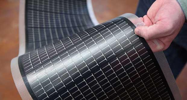
The preparation process of thin film solar cell modules typically involves several key steps. While there can be some variations depending on the specific technology used, the general process includes the following stages.
- Substrate preparation: A suitable substrate, often made of glass, stainless steel, or plastic, is prepared to serve as the base for the thin film layers.
- Cleaning: The substrate is thoroughly cleaned to ensure that it is free from any contaminants that could affect the performance of the solar cell.
- Deposition of layers: Thin film solar cells are composed of several layers, each with a specific function. The following deposition techniques are commonly used:
- Chemical vapor deposition (CVD): This process involves the deposition of thin layers of materials through the reaction of various gases on the substrate surface.
- Physical vapor deposition (PVD): PVD techniques include thermal evaporation and sputtering, which are used to deposit thin films of materials onto the substrate.
- Spray pyrolysis: This technique involves the deposition of thin films by spraying a precursor solution onto the heated substrate, followed by pyrolysis to form the desired thin film.
- Semiconductor layer deposition: The semiconductor layer is crucial for the conversion of sunlight into electricity. Commonly used materials for the semiconductor layer include amorphous silicon (a-Si), cadmium telluride (CdTe), and copper indium gallium selenide (CIGS). These materials are deposited onto the substrate using the techniques mentioned above.
- Transparent conducting oxide (TCO) deposition: TCO layers are applied to facilitate the extraction of generated electrical charges. Typically, materials like indium tin oxide (ITO) or fluorine-doped tin oxide (FTO) are used for this purpose.
- Back contact deposition: The back contact is another essential layer that is typically made of materials like aluminum or stainless steel. It is deposited to create a conductive layer that collects the electrons generated by the semiconductor layer.
- Encapsulation: To protect the thin film solar cells from environmental factors such as moisture, dust, and mechanical stress, encapsulation layers are added. These layers can be made of materials like glass or polymers, which are applied over the entire module.
- Wiring and connection: Electrical connections are made to allow the generated electricity to be collected and transmitted to an external circuit.
- Testing and quality control: The prepared thin film solar cell modules undergo rigorous testing to ensure that they meet specific performance criteria and quality standards.
This general process provides an overview of the steps involved in the preparation of thin film solar cell modules. However, it is essential to note that the specific details may vary depending on the type of thin film technology being used.